|
|||||||||||

High Temperature Superconductor Research at the Materials Departement of the ETH Zurich
Research at the Nonmetallic Inorganic Materials on high temperature superconductors is in co-operation with ABB corporate research Switzerland and is devoted to the development of the fault current limiter. The most promising high temperature superconductor compound for power applications is Bi-2212 for it can be processed as polycrystalline thick films and bulk material by the partial melt process. We focused on the production of large area thick films on novel substrate material and recently on the precursor production. Besides this applied research the Bi-Sr-Ca-Cu-O-Ag system was thermodynamically modelled, the pathway of the supercurrent was monitored and a novel superconducting compound was exploited.
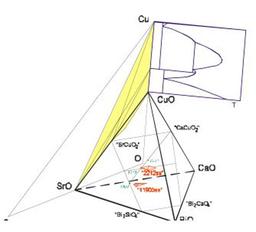
The thermodynamic modelling was conducted by the CALPHAD method and has brought deep insight into the phases and melt present in the Bi-Sr-Ca-Cu-O-Ag system. Although the composition of the superconductor is 2:2:1:2 the system can locally be far away from this stoichiometry especially during calcination or in the high temperature state. We have established the only complete and consistent thermodynamic description of all 56 solid phases and liquids of the system Bi-Sr-Ca-Cu-Ag-O.
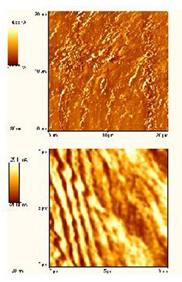
The current carrying capacity of Bi-2212 is limited by the cross-section of a material and not by the pinning of flux lines. The superconducting grqins could be imaged by MFM techniques. The current preferentially flows in regions near the grain boundary. Because of the poor pinning properties of the compound the grain boundaries are presumably the main pinning force in the material.
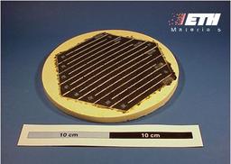
Bi-2212 is processed on Ag substrates, because the reactivity of the melt present in the high temperature state is very high. Alternatives to Ag are MgO. A series of polycrystalline oxide substrate materials were evaluated of which only MgO did not show any reactivity with the melt and does not poison Bi-2212. The production of large area and dense substrates was possible and Bi-2212 meanders were processed to thick film material yielding critical current densities exeeding 3000 A/cm2.
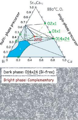
The production of high temperature superconducting components is based on processing of precursor materials. The critical current density is very sensitive to the precursor properties. Precursor properties can be correlated to the critical current density of fully processed material. The results lead to the hypothesis that the homogeneity of the peritectic decomposition throughout the device during partial melt processing is crucial. Therefore not the secondary phase content but its morphology and distribution has an influence on jc. It has been shown that secondary phases in the precursor are in fact beneficial to achieve high jc devices by acting as nucleation sites for the decomposition. The secondary phase formation can be influenced by the reaction pathway, calcination parameters and atmosphere control. Bi-2212 specimens have been produced from novel precursors of nominal 2212 stoichiometry but not of Bi-2212 phase composition yielding critical current densities of up to 8000 A/cm2 (10 µV/cm).
References
- Lang, T., Buhl, D. and Gauckler, L.J. (1998), "Influence of the Maximum Temperature during Partial Melt-Processing of Bi-2212 Thick Films on Microstructure and Jc.", Physica C 294 (1-2): 7-16.
- Buhl, D., Lang, T. and Gauckler, L.J. (1997), "Critical Current Density of Bi-2212 Thick Films Processed by Partial Melting.", Supercond. Sci. Technol. 10 (1): 32-40.
- Lang, T., Buhl, D., Al-Wakeel, S., Schneider, D. and Gauckler, L.J. (1997), "Phase Assemblage and Morphology during the Partial Melt Processing of Bi-2212 Thick Films.", Physica C 281 (4): 283-292.
- Lang, T., Buhl, D. and Gauckler, L.J. (1997). "Sample-Substrate-Interactions during Melting of Bi-2212 on Ag.", Supercond. Sci. Technol. 10 (5): 311-317.
- Lang, T., Buhl, D. and Gauckler, L.J. (1997), "Melting of Bi-2212 under Controlled Oxygen Partial Pressure with Silver.", Physica C 275 (3/4): 284-292.
- Lang, T., Buhl, D., Schneider, D., Al-Wakeel, S. and Gauckler, L.J. (1997), "Texture in Melt Processed Bi-2212." J. Electroceram. 1(2): 133-144.
- Buhl, D., Lang, T., Cantoni, M., Risold, D., Hallstedt, B. and Gauckler, L.J.(1996), "Critical current densities in Bi-2212 thick films.", Physica C 257 (1-2): 151-159.
- Buhl, D., Lang, T. and Gauckler, L.J. (1996), "Phase composition and grain alignment in partial melt processed Bi-2212 thick films.", Appl. Supercond. 4(7-8): 299-317.
- Lang, T., Buhl, D., Wu, Z., Schneider, D., Cantoni, M., Al-Wakeel, S. and Gauckler, L.J.(1996), "Gefügeentwicklung beim partiellen Schmelzen von Hochtemperatursupraleitern.", Oberflächen Werkstoffe 5: 17-20.
- Buhl, D., Lang, T., Heeb, B. and Gauckler, L.J. (1994), "Processing, Properties and Microstructure of Melt-Processed Bi-2212 Thick Films.", Physica C 235-240 : 3399-4000.
- Král, F., Kostorz, G., Ari, N., Gauckler, L.J., Perednis, D. and Han, K.-H. (1999), "Spatial and Force Resolution of Magnetic Force Microscopy in Current Imaging.", Czech. J. Phys. 49 (11): 1567-1574.
- Král, F., Perednis, D., Huey, B., Bonnell, D. A., Kostorz, G. and Gauckler, L.J. (1998), "Imaging Current Flow Distribution in Polycrystalline Bi2Sr2CaCu2Ox Superconductors by Magnetic Force Microscopy.", Adv. Mater. 10 (17): 1442-1448.
- Schneider, D., Köbel, S. and Gauckler, L.J. (2001), "Partial Melt-Processing and Annealing of (Bi,Pb)-1212 Superconductors.", Physica C 349 : 166-178.
- Schneider, D., Köbel, S., Gauckler, L.J.(2000), "Powder synthesis of (Bi, Pb)-1212 superconductors", Supercond Sci Techn 13 (10): 1476-1486.
- Köbel S, Nussbaumer R, Schneider D, et al. (2002), "Ceramic substrates for Bi2Sr2Ca1Cu2Ox melt-processing.", Physica C 377(4): 507-515.
Processing of Bi-2212 bulk components
The best method to prepare high-temperature superconducting devices of Bi2Sr2CaCu2Ox (Bi-2212), able to carry large transport currents at 77 K, is the partial melt process. During this heat-treatment the cuprate is melted and subsequently recrystallized upon controlled cooling. Almost all involved processing parameters have to be controlled within narrow limits in order to get good superconducting properties in the fully processed sample. We investigate the influence of the processing conditions on the microstructure and the superconducting properties of Bi-2212 thick films and bulk components covering the thickness range from 10 to 1000 µm.
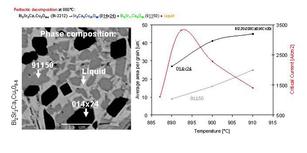
During partial melt processing of Bi-2212 a liquid and two solid phases are coexisting (91150 and 014x24) at high temperatures. Upon cooling grains of these two phases have to dissolve and lamellar grains of Bi-2212 recrystallize from the melt. These grains can easily be aligned in components of confined thickness up to 120 µm.
The key property of Bi-2212 power devices is the critical current density jc. All the processing parameters have an influence on jc. Some of the most crucial are the sample dimensions, the maximum procesing temperature, the holding time in the high temperature state, the cooling rate during recrystallisation and the atmospheres during the process.
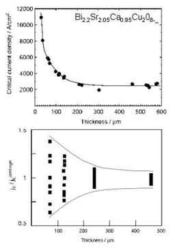
Experiments have shown that Bi-2212 grains do not grow larger than about 120 µm. Therefore the degree of texture is sensitiv to the sample thickness. However also the scattering of the jc increases with decreasing film thickness. This is due to inhomogeneous recrystallisation leading to agglomeration of undissolved secondary phases which reduce the current carrying cross section.
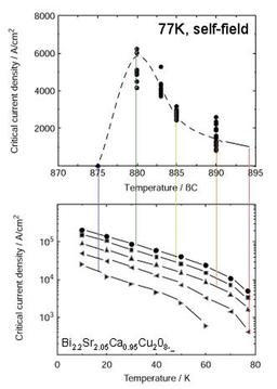
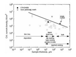
Material with high jc can only be achieved in a very narrow temperature intervall of the maximum processing temperature. This is mainly due to the rapid growth of the high temperature phases that then only partiallly redissolve. This correlation can be seen in the plots above and adjoining.
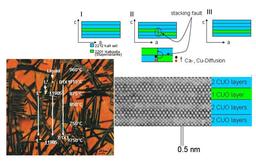
Depending on the cooling rate during recrystallisation from the high temperature state the amount of Bi-2201 intergrowths in the Bi-2212 can vary substantially. Atmosphere controll enables a reduction of the amount of intergrowth.
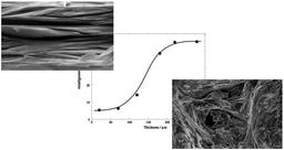
After partial melt processing the microstructures of the Bi-2212 will look as shown in the adjoining figures.
Critical current density of Bi-2212 is decreasing with component thickness. However, current carrying capacity per current lead width is increasing with thickness. Therefore, thicker material is of advantage in technical devices. The adjoining figure shows jc in dependence of the sample thickness over a wide range.
For more information, consult the papers by Schweizer, Müller, Bohac, Buhl, Lang, Kral, Köbel and Sager in our literature database.
Wichtiger Hinweis:
Diese Website wird in älteren Versionen von Netscape ohne
graphische Elemente dargestellt. Die Funktionalität der
Website ist aber trotzdem gewährleistet. Wenn Sie diese
Website regelmässig benutzen, empfehlen wir Ihnen, auf
Ihrem Computer einen aktuellen Browser zu installieren. Weitere
Informationen finden Sie auf
folgender
Seite.
Important Note:
The content in this site is accessible to any browser or
Internet device, however, some graphics will display correctly
only in the newer versions of Netscape. To get the most out of
our site we suggest you upgrade to a newer browser.
More
information

!!! Dieses Dokument stammt aus dem ETH Web-Archiv und wird nicht mehr gepflegt !!!
!!! This document is stored in the ETH Web archive and is no longer maintained !!!
!!! This document is stored in the ETH Web archive and is no longer maintained !!!